SMD components explained for PCB design, sourcing and assembly
What are SMD components?
SMD components are electronic parts designed to be mounted directly on the surface of a printed circuit board, rather than passing leads through drilled holes. The parts are surface-mount devices, while the manufacturing process is surface-mount technology, or SMT. For designers, buyers and technicians, an SMD part is not defined only by its electrical value. Package size, termination style, pad layout, moisture rating, heat path and assembly tolerance all affect whether it will work reliably on a real board. This guide explains the practical differences among common SMD components and connects them to PCB layout, sourcing and assembly decisions. For related background topics, visit the Components section.
SMD parts are widely used because they support compact layouts and automated assembly. Pick-and-place machines can place many small parts quickly, and reflow soldering can join hundreds or thousands of terminations in one controlled thermal process. Shorter interconnects can also help in high-speed and high-frequency circuits. The trade-off is tighter process margin. A wrong footprint, ambiguous size code or unsuitable soldering profile can turn a simple resistor or capacitor into a board-level reliability problem.
Common SMD component types
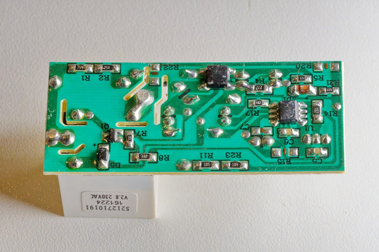
The term SMD components covers many device families. Passive chip components are the most familiar: resistors, multilayer ceramic capacitors, inductors, ferrite beads, thermistors and chip fuses. They usually have rectangular bodies with metallized end terminations. These packages are straightforward to place, but they still need correct pad geometry and suitable derating for power, voltage or current.
Semiconductor SMD packages include diodes, LEDs, transistors, MOSFETs, voltage regulators, logic devices, microcontrollers, memory and sensors. Their package names are more varied because the package must support pin count, heat dissipation, signal integrity and inspection requirements. Small-outline packages, SOT packages, QFN packages, DFN packages, BGA packages and wafer-level packages all address different mechanical and electrical needs.
Electromechanical and interconnect parts can also be surface-mounted. Examples include connectors, switches, microphones, antennas, shields and board-level modules. These parts may look simple in a bill of materials, but they can place higher demands on solder-joint strength, coplanarity, pick-and-place clearance and mechanical reinforcement. A USB connector, for example, should be evaluated not only by pin pitch but also by mounting tabs, insertion force, board-edge position and expected cable stress.
SMD package sizes and naming traps
One common source of confusion is the package-size code used for two-terminal chip parts. Codes such as 0402, 0603 and 0805 are often treated as universal, but the same number can refer to different dimensions depending on whether the code is imperial or metric. In everyday component distribution, many designers use imperial codes for common chip resistors and capacitors. However, many data sheets and CAD libraries also show metric equivalents. The safe approach is to confirm the actual body dimensions in millimeters, not just the numeric code.
| Imperial code | Metric code | Nominal body size | Practical note |
|---|---|---|---|
| 01005 | 0402 | 0.4 mm × 0.2 mm | Very small; usually requires advanced assembly control |
| 0201 | 0603 | 0.6 mm × 0.3 mm | Compact but harder to prototype and inspect |
| 0402 | 1005 | 1.0 mm × 0.5 mm | Common in dense commercial electronics |
| 0603 | 1608 | 1.6 mm × 0.8 mm | Often a good balance for automated assembly |
| 0805 | 2012 | 2.0 mm × 1.25 mm | Easier to handle and inspect than smaller chip sizes |
| 1206 | 3216 | 3.2 mm × 1.6 mm | Useful where power, voltage or manual work matters |
These dimensions are nominal. Real components have manufacturing tolerances, termination variations and height differences. The footprint must match the exact component series, not only the size family. A 0603 resistor, a 0603 capacitor and a 0603 ferrite bead may share similar length and width, while their thickness, recommended pad dimensions and solder volume can still differ.
Integrated-circuit packages create a different naming problem. Terms such as SOIC, TSSOP, QFN and BGA describe general package families, not a complete footprint. Pin count, pitch, body size, exposed pad dimensions and thermal-pad recommendations must all be checked. A 32-pin QFN from one manufacturer is not automatically interchangeable with another 32-pin QFN unless the mechanical drawing, pinout and land pattern match.
How SMD choices affect PCB layout
PCB layout is where an SMD selection becomes a manufacturable design. IPC-7351B is widely referenced for surface-mount land-pattern principles, and manufacturer data sheets often provide recommended pads for specific parts. When both are available, the data sheet should normally be checked first because it reflects the manufacturer’s actual package outline and soldering recommendation. IPC-style rules are especially useful when a library must be created consistently across many generic packages.
The land pattern controls solder-joint shape, self-alignment and inspection visibility. Pads that are too small may not provide enough solderable area. Pads that are too large can pull parts out of alignment or create excessive solder fillets. For fine-pitch ICs, solder-mask registration and stencil aperture design become as important as copper geometry. For QFN and DFN packages with exposed thermal pads, uncontrolled solder volume under the center pad can lift the package and weaken the outer leads.
SMD size also affects routing. Smaller passives free board area and can reduce loop length around decoupling networks, filters and high-speed signal paths. The limit is manufacturability. Aggressive miniaturization may reduce assembly yield margin, weaken probe access and make rework harder. In a prototype or low-volume design, moving from 0402 to 0603 or 0805 can reduce handling difficulty without changing the circuit concept. In a dense production device, the smaller size may be justified by board area, signal path and enclosure constraints.
Thermal design should be considered early. A power resistor, switching regulator, LED or MOSFET may be available in a compact package, but the board copper often determines whether it can dissipate heat safely. Exposed pads, thermal vias, copper pours and airflow can matter more than the package name alone. The same principle applies to current-carrying connectors and protection devices: the footprint and copper width must support the expected electrical and mechanical stress.
Assembly and reliability considerations
Most SMD assemblies use solder paste printing, automated placement and reflow soldering. The process is efficient, but it depends on a compatible combination of solder paste, stencil design, component finish, PCB finish and thermal profile. Very small passives can tombstone if one end wets before the other. Fine-pitch ICs can bridge if the paste deposit is too large or if pad design is poor. BGA joints are hidden under the package, so X-ray inspection may be needed for production verification.
Moisture sensitivity is another important issue for many nonhermetic semiconductor packages. IPC/JEDEC J-STD-020 defines moisture and reflow sensitivity classification for nonhermetic solid-state surface-mount devices. In practical terms, the moisture sensitivity level shown on packaging or in a data sheet tells assemblers how long the device can remain exposed to factory conditions before reflow and whether baking or dry storage is required. Ignoring this rating can lead to internal package damage during reflow even if the board looks acceptable from the outside. See also: Gadgets.
Inspection standards and acceptance criteria are also part of reliability. IPC-A-610 is commonly used in the electronics industry to describe acceptability of electronic assemblies, while IPC J-STD-001 addresses requirements for soldered electrical and electronic assemblies. A designer does not need to memorize every clause to choose a resistor or IC, but documented workmanship criteria help explain why footprint quality, solder fillet shape and component orientation matter.
Rework is possible for many SMD components, but the level of difficulty varies sharply. 0805 and 0603 passives can often be replaced with common tools by an experienced technician. Fine-pitch QFPs, QFNs, BGAs and tiny 01005 parts require tighter process control. Rework can also damage pads or surrounding parts if thermal mass, adhesive, underfill or shielding is not considered. For boards expected to need field repair or lab modification, package choice should reflect serviceability as well as density.
How to choose SMD components for a design
A sound SMD selection process starts with the circuit requirement, but it should not stop at electrical parameters. Treat the component, package, footprint and assembly process as one system. A part that looks equivalent in a schematic may be unsuitable if it is unavailable, has a different pinout, requires a difficult footprint or exceeds the assembler’s normal capability.
- Confirm electrical limits first. Check voltage, current, tolerance, temperature range, power rating, frequency behavior and derating notes.
- Verify the exact package. Compare body size, height, pitch, termination style, exposed pad and recommended land pattern.
- Use manufacturer footprint data when available. If a generic IPC-based footprint is used, compare it against the data sheet drawing.
- Match package size to assembly capability. Ask whether the assembler routinely places the selected size, especially for 0201, 01005, fine-pitch QFN or BGA packages.
- Consider inspection and test access. Small packages can save area, but they may reduce probe access and make visual inspection harder.
- Plan alternates carefully. Alternate parts should match not only value and rating but also package, pinout, height and supply-chain constraints.
- Review thermal and mechanical stress. Power parts, connectors and controls may need more copper, stronger pads or through-hole reinforcement.
Capacitors deserve special attention. A small multilayer ceramic capacitor may have the same nominal capacitance as a larger one, but real capacitance can vary with voltage, dielectric type, temperature and package size. Resistors also need derating for power and temperature. Inductors and ferrite beads should be checked for current rating, impedance curve, saturation and DC resistance. The package code is only a starting point; the data sheet determines whether the part is suitable.
Practical mistakes to avoid
The first mistake is copying footprints from an old library without checking the current data sheet. Component manufacturers can offer multiple package variants under similar ordering codes, and footprint recommendations can differ by series. The second mistake is mixing imperial and metric size codes in purchasing notes, CAD libraries or assembly drawings. Always include millimeter dimensions or the manufacturer’s package code when ambiguity is possible.
The third mistake is assuming smaller is always better. Smaller SMD components can improve density, but they can also reduce power margin, increase handling difficulty and raise assembly cost. A fourth mistake is ignoring height. Enclosure clearance, shielding cans, heat sinks, connectors and stacked boards can fail mechanically even when the PCB footprint is correct. Finally, avoid selecting a package that only one supplier can provide unless the design has a strong reason to accept that sourcing risk.
Frequently asked questions
What does SMD stand for?
SMD stands for surface-mount device. It refers to an electronic component designed to be soldered to pads on the surface of a PCB. SMT, or surface-mount technology, refers to the process used to assemble those parts onto the board.
Is 0603 an imperial or metric size?
It can be either, which is why it causes confusion. In common imperial chip sizing, 0603 means about 1.6 mm × 0.8 mm and corresponds to metric 1608. In metric sizing, 0603 means about 0.6 mm × 0.3 mm and corresponds roughly to imperial 0201. Always confirm the dimensions.
Are SMD components less reliable than through-hole parts?
Not inherently. Properly designed and assembled SMD joints can be highly reliable. Through-hole parts still have advantages where strong mechanical anchoring is needed, such as heavy connectors or components exposed to repeated force. The better choice depends on electrical, mechanical and manufacturing requirements.
Can SMD components be soldered by hand?
Many larger SMD parts, such as 0805 passives, SOIC packages and some connectors, can be hand-soldered with suitable tools and skill. Very small chips, fine-pitch packages, QFNs and BGAs are much harder and are usually better handled with controlled reflow, hot air, microscope inspection or specialized equipment.
What is the most important rule when selecting SMD components?
Do not select by electrical value alone. Confirm the package drawing, recommended footprint, availability, assembly limits, thermal behavior and inspection requirements before releasing the PCB. Most avoidable SMD problems come from treating the symbol, footprint and real component as if they were automatically interchangeable.