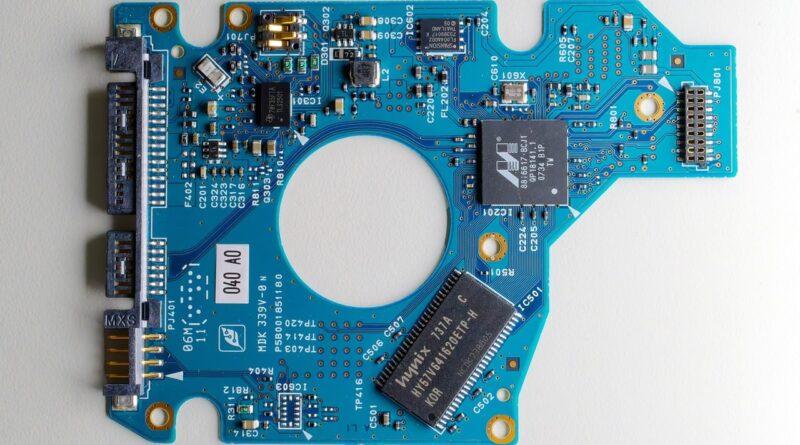
SMD components list for PCB design, package selection and sourcing
What belongs on an SMD components list?
An SMD components list is a structured reference for parts mounted directly on a printed circuit board using surface mount technology. For PCB designers, buyers and repair technicians, a useful list is more than a catalog of part names. It should connect each component type with common package styles, key electrical ratings, polarity or orientation risks, assembly limits and sourcing notes. The main groups are passive components, discrete semiconductors, integrated circuits, protection parts, timing and RF parts, and electromechanical devices such as switches and connectors.
This guide focuses on practical identification and selection rather than every package ever registered. It also explains why the package code, PCB footprint and datasheet confirmation matter as much as the component value itself. For related electronics references, visit the Components section.
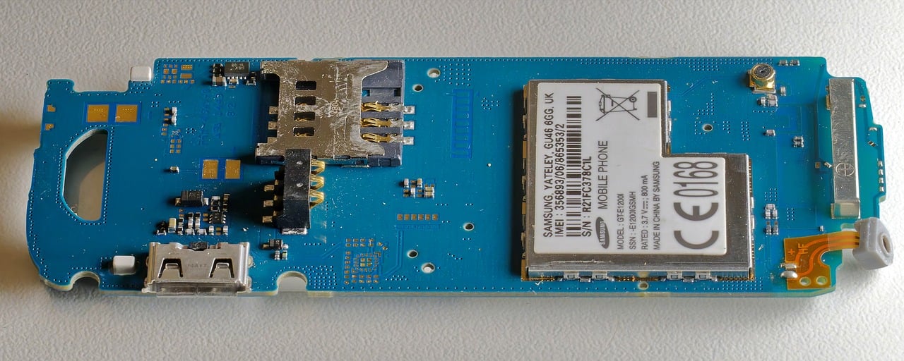
Core SMD component categories
Most surface mount bills of materials can be organized into a few repeatable categories. The table below provides a working list for common PCB design, repair and sourcing tasks.
| Category | Common SMD components | Typical package examples | Main selection points |
|---|---|---|---|
| Passive components | Resistors, capacitors, inductors, ferrite beads | 01005, 0201, 0402, 0603, 0805, 1206, 1210, 1812, 2512 | Value, tolerance, voltage, power, current, temperature coefficient, dielectric or core material |
| Protection components | TVS diodes, varistors, fuses, resettable PTCs, ESD arrays | 0402 to 1206 chips, SOD, SOT, DFN, QFN | Clamping voltage, surge rating, capacitance, hold current, response time |
| Discrete semiconductors | Diodes, Zener diodes, Schottky diodes, BJTs, MOSFETs, LEDs | SOD-123, SOD-323, SOT-23, SOT-223, SC-70, TO-252, TO-263 | Polarity, voltage, current, leakage, switching speed, thermal resistance |
| Integrated circuits | Op amps, logic ICs, regulators, MCUs, sensors, memory, drivers, RF ICs | SOIC, SOP, TSSOP, MSOP, SSOP, QFN, DFN, LGA, BGA, WLCSP | Pin count, pitch, thermal pad, moisture sensitivity, programming and test access |
| Timing and frequency parts | Crystals, oscillators, resonators, SAW filters, RF filters | 2-pad and 4-pad ceramic SMD, metal can SMD, QFN-like modules | Frequency, load capacitance, ppm tolerance, aging, drive level, layout sensitivity |
| Electromechanical parts | Connectors, switches, relays, microphones, antennas, shields | Custom SMD footprints, gull-wing leads, castellation, bottom contacts | Mechanical retention, height, mating cycles, orientation, keep-out zones |
Package names and dimensions vary by manufacturer. A regulator in SOT-223, for example, creates a very different layout and thermal problem from the same function in a small DFN. Treat the package as part of the component identity, not as a minor detail added after schematic design.
Passive SMD components and common chip sizes
Passive parts are the most numerous SMD components on many boards. The familiar four-digit codes for rectangular chips usually describe nominal body length and width. In the widely used imperial convention, 0603 means about 0.06 by 0.03 inches, commonly listed as approximately 1.6 by 0.8 mm. Datasheets may also show a metric code, so designers must confirm which naming system is being used before selecting a footprint.
| Imperial chip code | Approximate metric body size | Common uses | Practical notes |
|---|---|---|---|
| 01005 | 0.4 x 0.2 mm | Very dense mobile and module designs | Difficult for hand assembly and visual inspection |
| 0201 | 0.6 x 0.3 mm | Compact consumer electronics and RF sections | Requires tight placement and stencil control |
| 0402 | 1.0 x 0.5 mm | Dense digital, analog and RF boards | Common in production, still challenging for manual rework |
| 0603 | 1.6 x 0.8 mm | General-purpose resistors, capacitors and ferrite beads | Good balance of size, availability and assembly tolerance |
| 0805 | 2.0 x 1.25 mm | Decoupling, pullups, filters, indicators | Easier to prototype and inspect than smaller chips |
| 1206 | 3.2 x 1.6 mm | Higher power resistors, larger MLCCs, fuses | Often chosen when voltage, power or capacitance needs increase |
| 1210 and larger | 3.2 x 2.5 mm and above | Power, surge, high-capacitance and protection parts | Board area increases, but electrical and thermal margins may improve |
SMD resistors
SMD resistors are selected by resistance value, tolerance, rated power, voltage rating, temperature coefficient and package size. A 10 kΩ resistor in 0402, 0603 and 1206 may look equivalent in the schematic, but the larger package generally offers better power dissipation and easier handling. Precision analog circuits may also require a low temperature coefficient and low noise specifications, not only a tight tolerance.
SMD capacitors
SMD capacitors include ceramic MLCCs, tantalum, polymer, aluminum electrolytic and film types. MLCCs are widely used for decoupling and filtering, but package size, dielectric class, voltage rating and DC bias behavior can change the effective capacitance in operation. For this reason, a 10 µF 0603 MLCC and a 10 µF 1206 MLCC may not behave the same in a powered circuit.
SMD inductors and ferrite beads
Inductors and ferrite beads may use rectangular chip packages, molded packages or shielded power inductor bodies. Important parameters include inductance, rated current, saturation current, DC resistance, impedance versus frequency and shielding. In switch-mode power supplies, the inductor affects heat and EMI performance as well as the electrical design.
Discrete semiconductor SMD components
Discrete semiconductors may be small in quantity, but they are important for power control, signal direction, switching and protection. Unlike many passive chips, most semiconductor packages are polarized or pin-dependent, so orientation marking must be clear in the PCB layout, assembly drawing and inspection process.
| Component type | Common packages | Where it is used | Watch points |
|---|---|---|---|
| Signal diode | SOD-123, SOD-323, SOD-523 | Clamping, steering, small-signal rectification | Polarity band, reverse voltage, recovery time |
| Zener diode | SOD, SOT-23 | Voltage reference and clamp circuits | Power derating and dynamic impedance |
| Schottky diode | SOD, SMA, SMB, SMC | Low-forward-voltage rectification | Leakage at temperature and reverse voltage margin |
| TVS diode | 0402 to 1206, SOD, DFN, arrays | ESD and surge protection | Capacitance, clamping voltage and placement near connector |
| BJT transistor | SOT-23, SOT-323, SOT-223 | Switching, level shifting, small amplifiers | Pinout variants and gain range |
| MOSFET | SOT-23, SO-8, PowerPAK-style, DFN, TO-252, TO-263 | Load switches, converters, motor and LED drivers | RDS(on), gate charge, thermal pad and safe operating area |
| LED | 0603, 0805, 1206, PLCC, high-power ceramic packages | Status indication and lighting | Polarity, brightness bin, color bin and current rating |
SOT-23 is one of the most familiar small-outline transistor packages, but it is not limited to transistors. Voltage references, small regulators, op amps, logic gates and sensors can also appear in SOT-23 variants with three to six pins. Always check the manufacturer pinout because the same outline can support different electrical arrangements.
Integrated circuit packages in an SMD components list
IC packages define how a device is assembled, routed, inspected and cooled. The same function may be available in a hand-solderable SOIC and in a compact QFN or BGA. The right choice depends on board density, signal speed, thermal requirements, assembly capability and rework strategy.
Leaded packages
SOIC, SOP, SSOP, TSSOP and MSOP packages have visible leads around the body. They are popular for logic, amplifiers, interfaces, regulators and controllers because they are easier to inspect and rework than many leadless packages. Pitch still matters: a 1.27 mm SOIC is much easier to hand solder than a fine-pitch TSSOP.
Leadless packages
QFN, DFN, SON and LGA packages save board area and can improve electrical performance by reducing lead length. Many include an exposed thermal pad under the body. That pad improves heat transfer, but it also adds layout, stencil, solder voiding and inspection considerations. For production boards, land pattern design and assembly notes should be reviewed before the footprint is released. See also: Gadgets.
Array packages
BGA, FBGA and WLCSP packages place solder balls or bumps under the device. They support high pin counts and compact routing, but they usually require controlled reflow, X-ray inspection for some defects and a more mature PCB fabrication process. They are not ideal for simple repair work unless the workshop has suitable equipment.
How to read package codes without choosing the wrong part
Package names are useful shortcuts, but they are not complete specifications. A reliable SMD list should separate at least four items: the electrical component type, the package outline, the manufacturer footprint recommendation and the ordering part number. Confusing any of these can lead to boards that assemble poorly or parts that do not fit.
- Check imperial versus metric chip codes. The code 0402 can describe different sizes if a datasheet uses metric naming instead of the imperial convention. Confirm the dimensions in millimeters before creating or downloading a footprint.
- Do not assume one SOT-23 pinout. Three-pin, five-pin and six-pin variants exist, and pin functions differ by device family.
- Compare land pattern recommendations. IPC land-pattern standards are useful references, but manufacturer datasheets may include package-specific tolerances, thermal pad dimensions or stencil notes.
- Watch height as well as length and width. Enclosures, shields, batteries and stacked boards can fail because of component height even when the PCB footprint is correct.
- Confirm tape-and-reel packaging. Placement orientation, reel quantity, moisture barrier packaging and minimum order quantity can affect assembly planning.
For professional PCB work, the footprint should be verified against the component datasheet, not only against a library name. Standards such as IPC-7351 and IPC-7352 are commonly used as land-pattern references, while JEDEC outlines and manufacturer package drawings help define physical package geometry. In practice, the datasheet remains the final authority for the exact part being placed.
Selection checklist for design and sourcing
A practical SMD components list becomes more valuable when it supports decisions. Use the checklist below before releasing a schematic, BOM or PCB library item.
- Define the electrical requirement. Record value, tolerance, voltage, current, frequency, speed, accuracy and environmental range.
- Select a realistic package size. Smaller is not always better. Consider assembly yield, rework, power dissipation, creepage, clearance and availability.
- Verify thermal performance. Power resistors, regulators, MOSFETs, LEDs and dense ICs need derating based on board copper, airflow and ambient temperature.
- Confirm polarity and orientation. Diodes, LEDs, electrolytic capacitors, tantalum capacitors, ICs and many modules must have clear markings on the silkscreen and assembly drawing.
- Check lifecycle and alternates. For production, avoid a single-source part when a generic value and package can work. For specialized ICs, list approved alternates only after electrical and footprint review.
- Match the assembler’s capability. Very small chips, fine-pitch QFNs, BGAs and WLCSPs require process control that may not be available in every prototype shop.
- Review compliance needs. RoHS, halogen-free status, automotive grade, moisture sensitivity level and operating temperature may be required depending on the product.
Frequently asked questions
What is the difference between SMD and SMT?
SMD means surface mount device, the component itself. SMT means surface mount technology, the assembly method used to place and solder those devices on a PCB. In casual use, people often say SMD components when they mean parts intended for SMT assembly.
What are the most common SMD passive sizes?
For general PCB work, 0402, 0603, 0805 and 1206 are among the most commonly encountered passive chip sizes. 0201 and 01005 are used in very dense designs, while 1210 and larger packages are common when higher voltage, current, capacitance, surge rating or power dissipation is needed.
Can I replace an SMD component with the same value in a different package?
Sometimes, but not automatically. The electrical value is only one requirement. The replacement must also match voltage, current, power, tolerance, temperature behavior, pinout, footprint, height and thermal performance. For polarized or active parts, package and pin assignment are critical.
Why do SMD package codes cause confusion?
Many rectangular chip codes originated from imperial dimensions, but metric codes also appear in datasheets and catalogs. The same number can refer to different physical sizes depending on the naming system, so the safest method is to confirm the millimeter dimensions and manufacturer drawing.
Which SMD packages are easiest for hand soldering?
Larger passive chips such as 0805 and 1206, SOD packages, SOT-23 and SOIC packages are generally easier for manual soldering than 0201 chips, fine-pitch TSSOPs, QFNs or BGAs. Skill, tools, flux, magnification and board finish also affect the result.